


There’s two cases when hackers have to think about USB-C connector mechanics. The first is when a USB-C connector physically breaks, and the second is when we need to put a connector on our own board. Let’s go through both of them.
Clean That Connector
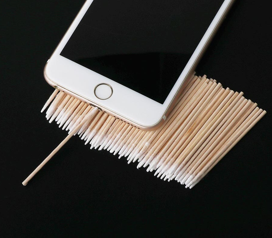 What if a socket on your phone or laptop fails? First off, it could be due to dust or debris. There’s swabs you can buy to clean a USB-C connector; perhaps adding some isopropyl alcohol or other cleaning-suitable liquids, you can get to a “good enough” state. You can also reflow pins on your connector, equipped with hot air or a sharp soldering iron tip, as well as some flux – when it comes to mechanical failures, this tends to remedy them, even for a short period of time.
How could a connector fail, exactly? Well, one of the pins could break off inside the plastic, or just get too dirty to make contact. Consider a device with a USB-C charging and data socket, with USB 2.0 but without high-speed pairs – which is to say, sadly, the majority of the phones out there. Try plugging it into a USB-A charger using a USB-A to USB-C cable. Does it charge, even if slowly? Then, your VBUS pins are okay.
Plug it into a Type-C charger using a Type-C cable, and now the CC pins are involved. Does it charge in both orientations? Then both of your CC pins are okay. Does it charge in only one orientation? One of the CC pins has to be busted. Then, you can check USB 2.0 pins, used for data transfer and legacy charging. Plug the phone into a computer using a USB-A to USB-C cable. Does it enumerate as a device? Does it enumerate in both orientations? If not, you might want to clean D- and D+ pins specifically, maybe even both sets.
Can Be Replaced – Sometimes
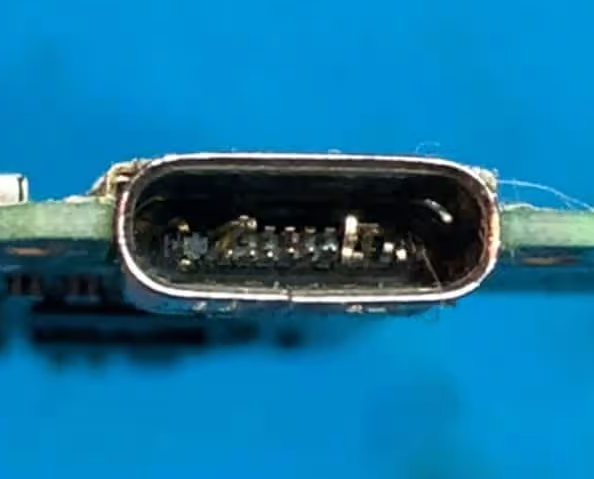 It also helps if you can take your device apart, get a USB-C plug breakout and measure continuity through the socket. What if your connector is too busted and there’s no continuity, no matter how much you reflow a specific pin? Well, it might be bad news, unless you own a reasonably popular device.
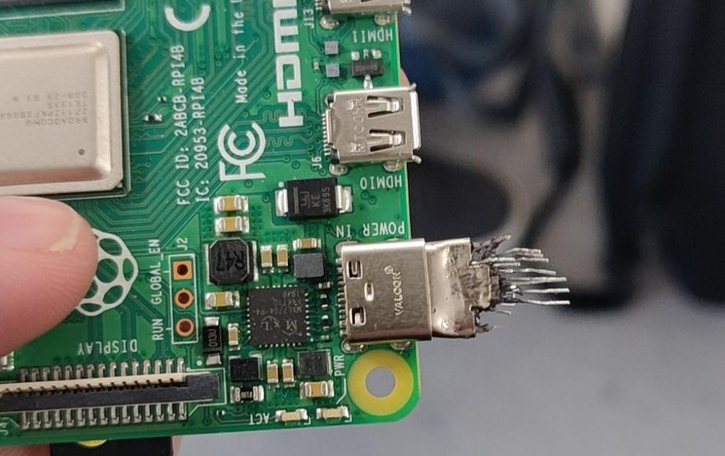
I would not be surprised if there’s literally a thousand different USB-C connectors types out there – and every phone and laptop under the sun seems to use a slightly different, mechanically incompatible one. If a USB-C connector in your expensive device fails, you might have to look for a very, very specific replacement part. They’re also often bothersome to desolder and replace, given that they’re always a combination of through-hole and SMD parts. Sometimes the SMD pads are firmly under the connector and inaccessible, and with edge-mount connectors, sometimes they’re on both sides of the board. Often, there’s plastic right next to the pins, or over them. All of this makes it bothersome to use hot air or a soldering iron for removing the connector.
On the upside, not all manufacturers are half-intentionally hostile like that. New Macbooks have USB-C sockets on a separate, easily detachable and replaceable part. Many phones have the USB-C port on a separate small PCB on the bottom of the phone, too. In both cases, you can just go on Aliexpress and purchase a separate board, that you then replace. Now, disassembling modern phones is a rabbit hole, but I guess we can be thankful that there’s at least there’s some consideration.
Just like MicroUSB, USB-C connectors have small latches. They’re not visible – as they’re inside the plug, on the sides. That said, they’re more often present than not. Of course, just like MicroUSB, these latches also wear out. Thankfully, all you need to do is to buy a different cable. And what if it’s your favourite cable, or what if you feel like building your own cables?
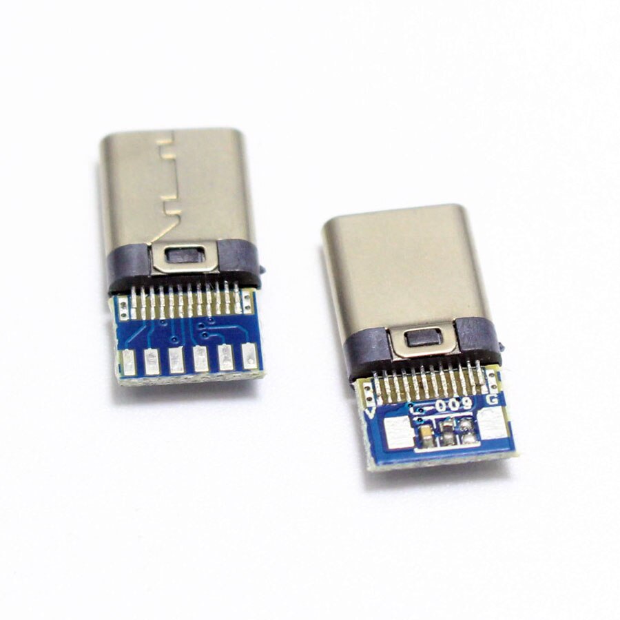
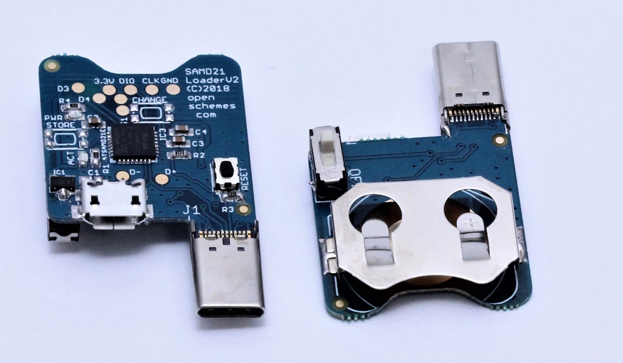
You can also buy USB-C plugs with small breakout PCBs, that let you solder wires onto them. Having such plugs lets you build custom cables or create new ones; I personally buy them from LCSC as they stock a surprising variety if you know where to search. There are plugs that have pullup resistors on them and will work great for building USB-A to USB-C cables, but you better be sure to remove the resistor for USB-C to USB-C applications. There are plugs that expose both CC pads, extra handy in case you want to build your own USB-C extensions or something. And there are also plugs with an emarker programmed, in case you want to get 5 A out of a PSU and need to build a custom cable, among other things.
By now, we’re firmly into the territory of making our own stuff. Let’s talk about doing it properly – again, limiting ourselves to mechanical aspects, for now.
General Connector Rules
For a start, let’s highlight something great about USB-C sockets. The overwhelming majority of them have through-hole mounting pins – a welcome departure from legacy of MicroUSB and MiniUSB, where the cheapest connectors you could buy were surface-mount only, making it easy to rip the connector off the board. It’s really hard to find a USB-C socket that’s fully surface-mount, and this does make things more mechanically sturdy.
For hackers, this does tend to make PCBs and assembly and bit pricier – you need your fab to be able to do PCB slots, since most USB-C connector footprints use slots, and when ordering PCBs with assembly, you have two or four extra through-hole pins that need to be manually soldered – which comes with extra fees. That said, it’s undoubtedly for the better, and prices will go down over time.
USB-C connectors, sockets and plugs alike, have current ratings. All the sockets are supposed to be rated for 5 A, but I’ve seen some Chinese ones rated for 3 A; check the datasheet. Of course, if you’re putting a 5 A connector on your board, remember that it will only pass 5 A if your board is able to request that, which in turn requires active USB-PD communications — the usual dual 5.1K pulldown arrangement isn’t sufficient for that. On the upside, if you’re not aiming to have a 5 A connector specifically, you don’t need to check the current rating.
This variety of sockets exists because there are myriad ways you might want to mount a USB-C socket – on top of the board horizontally, or vertically, or vertically but facing sideways, or inline with the board with dozens of possible heights, with or without waterproofing, and of different manufacturing quality. There’s also myriad ways to expose high-speed pairs, if you need a connector with those. Some use SMD pads and some use through-hole pins for high-speed, and that’s just scratching the surface.
Not all connectors are good for you, either – which does help decrease the variety somewhat. First of all, you will see connectors without CC pins exposed, which will only really work with USB-A to USB-C cables. One could expect to find such a connector in a “baby’s first soldering kit” package sold for $3. You really shouldn’t use them, however. There’s also plenty of connectors that expect to have SMD pads for pins fully hidden under their own package. If your solder paste stenciling skills aren’t up to snuff, you really, really don’t want to debug soldering issues with such connectors.
Low Speed, Simple Rules
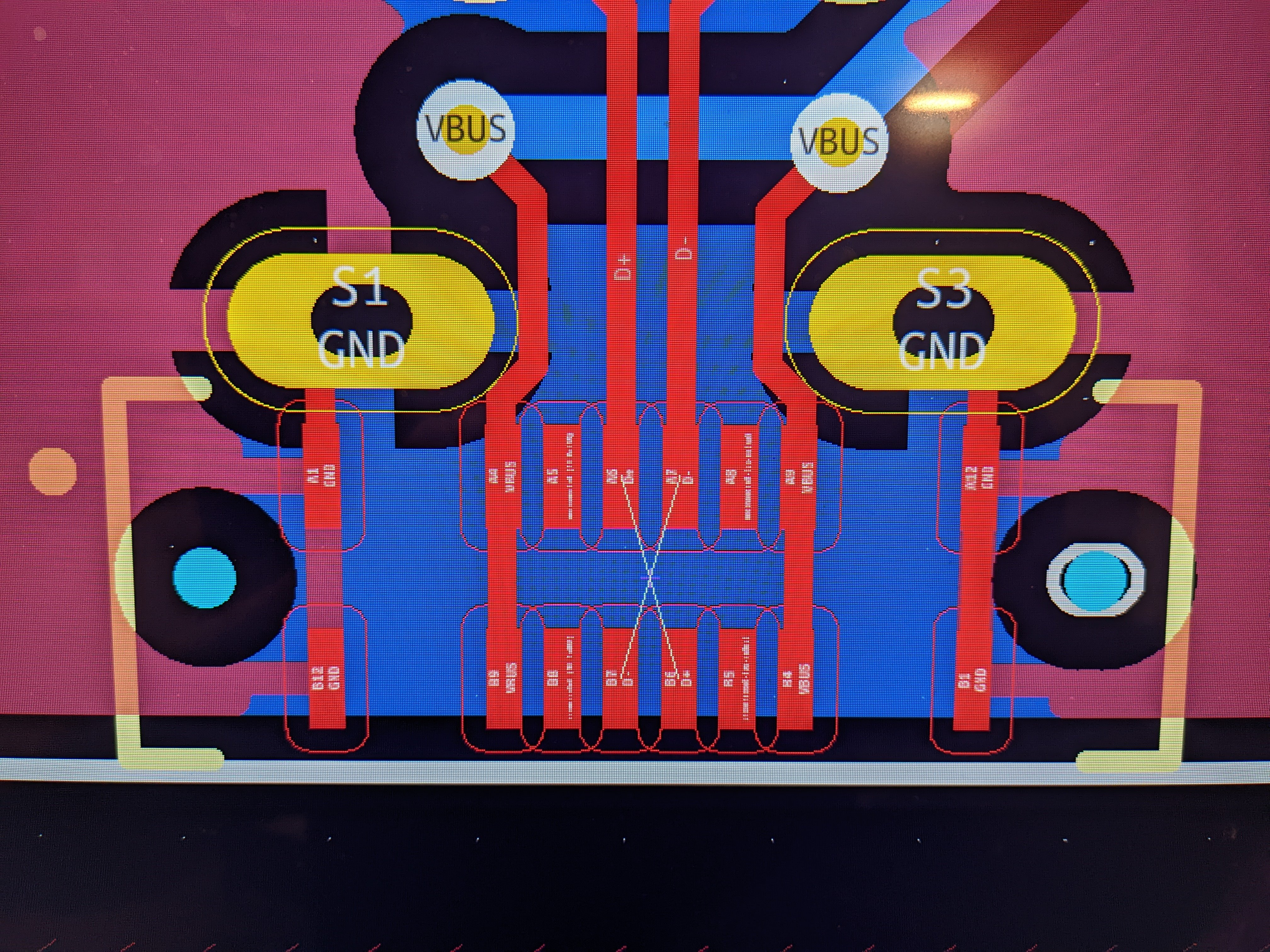
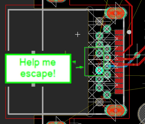
Let’s limit ourselves to USB 2.0 and CC, and of course, VBUS and GND. The hobbyist choice of a tried and true connector, highlighted in the first article, is the 16-pin SMD one. You will see it on devboards, cheap USB-C-equipped products, and many a hacker creation – it’s special in that it’s somewhat defined in the USB-C specification, too. KiCad has its footprint listed as USB_C_Receptacle_HRO_TYPE-C-31-M-12 with a matching symbol called USB_C_Receptacle_USB2.0, but HRO are certainly not the first to produce this connector, and there’s a trove of pin- and footprint-compatible connectors to this one specifically. Plus, as I mentioned, you get SBU pins, and you might want to use them for something like a UART – or perhaps, delete the SBU pads from the footprint so that you have two less pins you can possibly bridge during soldering, as the picture illustrates.
When you find a nice-looking substitute connector, do check its datasheet pin numbering with that of the PCB footprint you’re using. There’s been cases when in-datasheet footprint pin numbers are different from the commonly used numbers, or the datasheet was confusing and lead to hackers making mistakes, causing hours of debugging after a manufacturing issue has been found. While you’re in the datasheet, check if there’s a recommended PCB thickness for mounting such a connector. Even though such connectors mount on top of the board, PCB thickness might define how easy it’s going to be to have the shell pins solder properly. That said, it’s more of a recommendation than a requirement.
High Speed, High Demands
What if you ever want to use connectors with access to high-speed lanes? Sadly, I don’t have a specific high-speed connector to recommend you, but I I can certainly give you a few guidelines on how you can find one.
If you’re looking to settle on a high-speed-capable socket for your designs, I would recommend that you either find an existing and verified open-source design that looks easy to solder for you, or perhaps, find a few connectors that look suitable, order samples, design a board with test footprints for all of them, then try assembling a few and see how well it goes.
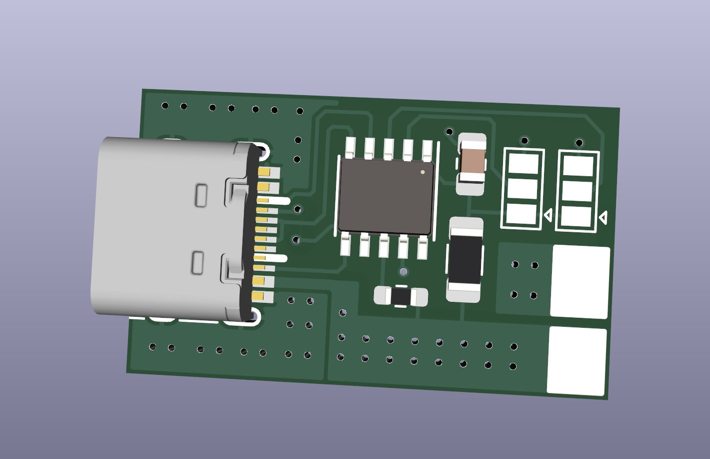
If you’ve found a footprint online that looks like it would fit a nice connector you found, check the dimensions carefully, then check again – even if the footprint name is the connector part number verbatim. Two months ago, I decided to make a breakout exposing all high-speed lanes on a USB-C socket, having the signals at least pretend to look like a differential pair. It’s not exactly close to being reasonably suited for actual day-to-day USB3 or DisplayPort use, since I ordered it as a two-layer board and the impedance is therefore out of wack, but it’s still better than the usual breakouts with 90 degree bend “high-speed” traces.
I found a footprint in KiCad that looked like it’d be easy enough to solder – through-hole pins for the row under the package, and surface-mount but soldering-iron-accessible pads for the row outside of the package. I found some connectors on LCSC that looked like they fit the footprint. When the day came to solder connectors onto breakouts, it turned out that the shield pins on the front were offset a few millimeters from the footprint locations. It also turned out that PCB holes for through-hole pins were just a tiny bit too tight after plating was added – next version will certainly have slightly larger holes.
Edges And Plugs
 It might be that you find a nice edge-mount connector with through-hole high-speed inner row pins. When doing PCB layout, you then might realize that it’s impossible to pull two of the innermost signals out – one CC and one SBU. One workaround is to straight up omit these two pins if the footprint is for a USB-C plug: you don’t use SBU and you don’t need a second pin for VCONN, which is, simply put, an unused CC pin reused as a power pin for an emarker.
Or you could solve the problem. The first way is to use a multi-layer board and route the pin out through an inner layer, where annular rings of through-hole pins aren’t present. The second way is using tracks tiny enough that they can still pass around the connector, by the PCB edge. Or for a third way, you could sneakily decrease the width of two through-hole pads around the offending pins on the top (non-solderable) layer, until a track fits between them.
Most of what I’ve mentioned applies to sockets and plugs equally. Of course, there are some plug-specific issues. For instance, there are mid-mount plugs – plugs that expose the full set of pins, with each USB-C pin side on different side of your PCB, and they’re reasonably nice to solder. On the other hand, I have no idea how such plugs are assembled at the factory – they seem to be reflowed and not manually soldered in products I’ve disassembled, but since there are SMD pads on both sides that the connector goes on top of, I have no idea how you would stencil such a board, especially in a larger-scale manufacturing environment. Any ideas?
Another peculiar consideration is that you’re only allowed to have a plug connect a single set of USB 2.0 data pins, which is to say, one pair of USB 2.0 pins has to stay disconnected. Some solderable plugs even have a second pair of USB 2.0 pins physically missing. I’m not quite sure why you can’t do this, especially given that almost every single USB-C socket PCB design parallels these pins, and it would just be a parallel connection all the same.
And that’s everything that you might want to know about USB-C connector mechanics. Of course, if I missed something, do talk about it in the comments!